Rehan Kapadia
Director MOSIS 2.0


| Foundry Service | Technology Node | Tapeout Date |
|---|---|---|
| TSMC | 65 nm | 11/18/2026 |
Rapid prototyping and process development capability through access to seven university nanofabrication facilities and other experimental prototyping facilities within the Southern California area and throughout the nation.
Supporting both silicon CMOS and advanced compound semiconductor technologies with seamless access to a wide array of commercial silicon MPW services from leading large, medium, and small-volume foundries.
Providing comprehensive chip design services that simplify and streamline the development process, enabling customers to bring their innovative ideas from concept to silicon.
The SWAP Hub provides a suite of test and modeling services to evaluate materials, devices, packages, and full systems across a wide range of environments for mission-critical applications.
Moscone Center
San Francisco, CA
October 13-15, 2026
MOSIS 2.0: Booth 221
Orlando World Center Marriott
Orlando, FL
October 21-24, 2026
MOSIS 2.0: Booth 11
Hilton San Francisco Union Square
San Francisco, CA
December 12-16, 2026
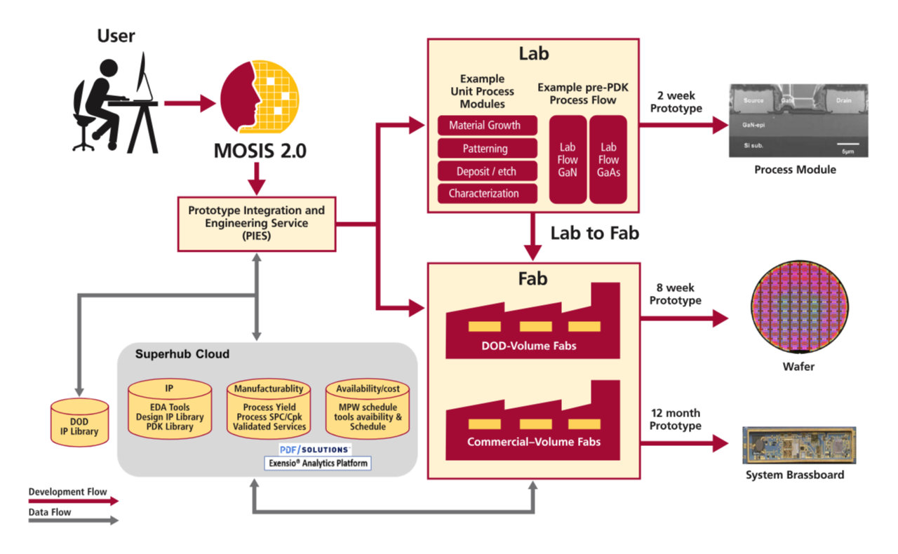
MOSIS 2.0 is the central storefront and gateway to access cutting-edge prototyping services, targeting advanced RF, 5G/6G, and EW applications.
The Prototype Integration and Engineering Service (PIES) Team is at the core of MOSIS 2.0 - a dedicated fab-knowledgeable engineering group that supports designers to accelerate their innovations to solutions.
We invite innovators, researchers, and industry partners to engage with MOSIS 2.0-and join us in advancing next-generation microelectronics.
Director MOSIS 2.0
Fab Prototyping Services Manager

Senior Project Manager

Microelectronics Fabrication Engineering Manager
Receive notifications for new MOSIS 2.0 offerings and upcoming MPW runs.
📅 March 10 | 3:30–5:30 PM CST
📍 Hilton Garden Inn, New Orleans Convention Center
Discover how MOSIS 2.0 can be your one-stop shop for access to MPW runs, research fabs, and expert design support.
👉 Register your interest now:� https://lnkd.in/gRVCw88a
Also find us at booth 412 at the GOMACTech Exhibition.
📍 Hilton Garden Inn – New Orleans Convention Center
📅 March 10 | 3:30 – 5:30 PM CST
This workshop is designed for semiconductor and microelectronics developers looking to accelerate circuit design and prototyping — from concept to tape-out.
Engage directly with the MOSIS 2.0 team and explore how to streamline your development cycle and bring advanced microelectronic systems to life faster.
Seats are limited.
👉 Express your interest here: https://lnkd.in/gRVCw88a
You can also chat with us at booth 412 at the GOMACHTech exhibition. We look forward to meeting you!